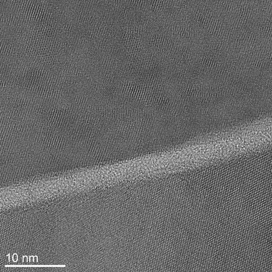
High-Resolution Transmission Electron Microscopy (TEM) Imaging
Transmission electron microscopy (TEM) is the highest-resolution imaging technique available today.
It is used to visualize sample features with atomic-level spatial resolution limits to characterize the morphology of complex nanostructures.
Get Expert Analysis of Your Material
How Transmission Electron Microscopy (SEM) Works?
In a TEM, a high-energy electron beam is applied to a very-thin sample (a lamella), which is prepared to be electron-transmissive i.e. typically 20 to 50 nm thick.
As the beam passes through the sample, scattering interactions occur between its electrons and the atoms present which alter the transmitted beam intensity. These scattering events can produce several types of contrast in the final image, including: amplitude contrast (arising from atomic number and mass/thickness) phase contrast (from quantum phase shifting due to multiple scattered beams’ interference), diffraction contrast (from crystal structure and orientation), and more.
Different imaging modes on the TEM can target certain types of contrast over others, facilitating specialized analysis of relevant information.
The electron beams transmitted through the sample are focused by the TEM objective lens to form an image below it. This image is then magnified through a final series of electromagnetic optics, and detected by a specialized CCD camera.
Our Process
Prepare Sample
Thin lamella (~20–50 nm) made with FIB-SEM.
Beam Imaging
High-energy electron beam passes through sample, generating contrast.
Image Capture
Electrons are focused, magnified, and recorded by a high-resolution detector.
Analyze Data
Structural and chemical insights from imaging modes + EDS/EELS/tomography.
TEM Instrument Used
ThermoFisher Scientific Talos F200X (S)TEM
TEM Line Resolution: ≤ 0.10 nm
TEM Information Limit: ≤ 0.12 nm
Maximum Alpha Tilt: ± 90° (with tomography holder)
Maximum Diffraction Angle: 24°
Electron Source: High-Brightness Field Emission Gun
Gatan OneView CCD: 16MP 4K camera
Quad-EDS Detectors for enhanced sensitivity and detection limits
Strengths
Highest possible spatial resolution: limit is atomic-scale
Bright Field and Dark Field imaging
Distinct imaging modes allow isolation of certain types of contrast information
Compatible with chemical (EDS) analysis and electrochemical analysis (EELS) techniques
Tomography and 3D reconstruction
Limitations
Requires extensive sample prep (normally performed with aFIB-SEM)
Specimens can be damaged if low dose techniques are not employed
Minimal topographical sensitivity
Typically only able to image a very small portion of the sample
Your Material Analysis Begins Here
Our team of experts is ready to provide a detailed and accurate quote tailored to your specific project requirements

.svg)
.svg)