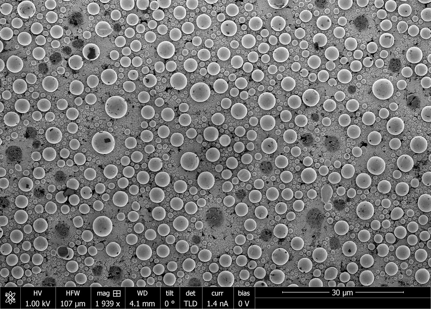
SEM analysis can produce images with resolutions below 1 nanometer (nm), and large depths of field to highlight surface topography and sample morphology.
A Scanning Electron Microscope (SEM) scans the surface of solid samples living and nonliving by rastering a high-energy electron beam. Because of the high accelerating voltage used to power the electron beam, SEMs yield resolution limits orders-of-magnitude improved over conventional light-based microscopes.
Get Expert Analysis of Your Material
What is Scanning Electron Microscopy (SEM)?
When performing Scanning Electron Microscopy Analysis, a high-energy electron beam is projected onto the surface of a solid sample (composed of conductive materials such as metals or composites), ejecting electrons, X-rays and photons used to produce high-resolution images and other details information about the specimen.
Capable of achieving a magnification range as high as 100,000x. SEM analysis offers remarkable insights into a material's chemistry and structure, combining both morphology and elemental composition data. Insights from SEM Analysis are paramount to advanced materials research across industries ranging from aerospace to personal electronics.
Our Process
Sample Preparation
Mount samples on SEM stubs. Apply a conductive coating (e.g., gold or platinum) to non-conductive materials to reduce charging.
SEM imaging
Scan the sample with a focused electron beam in vacuum. Collect SE for surface detail, BSE for compositional contrast, and EDS for elemental data.
Multi-Modal Acquisition
Capture images using multiple modes (SE, BSE, EDS). Optional enhancements include CL for luminescence and in-lens SE for finer resolution.
Analysis & Reporting
Interpret structural and elemental features. Deliver a report with imaging parameters, annotated images, and key findings.
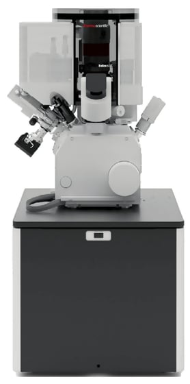
ThermoFisher Scientific Helios 5 UC (x3)
A specific model of an SEM manufactured by Thermo Fisher Scientific, the ThermoFisher Scientific Helios 5 UC (x3), incorporates DualBeam technology, advanced electron optics, and high current abilities using a Gallium (GA) source.
Maximum Horizontal Field Width: 2.3 mm at 4 mm WD
Electron Beam:
Resolution Limit: 0.7 nm at 1 kV
Current Range: 0.8 pA to 100 nA
Accelerating Voltage Range: 350 V to 30 kV
Ion Beam
Resolution Limit: 4.0 nm at 30 kV using preferred statistical method
Current Range: 1 pA to 100 nA
Accelerating Voltage Range: 500 V to 30k
Strengths
High-resolution imaging
Precise compositional analysis
Versatility among various scientific industries
Non-destructive analysis (allows repeated analysis of the same sample)
Provides topographical and crystallographic information about material structure
Indispensable aid in gaining an in-depth understanding of material properties
Limitations
Cannot deliver information about the internal structure of samples
Operating in a vacuum chamber hinders the analysis of gases or liquids
May introduce image distortions due to charging effects on non-conductive samples
Ready to unlock detailed insights into your materials?